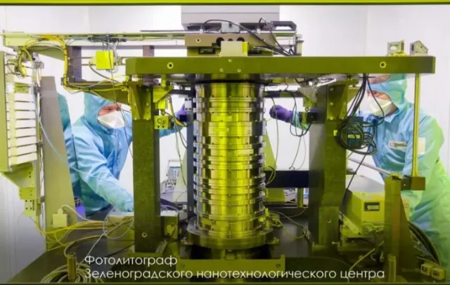
The development of domestic lithographs, interrupted in 1991 at the technological level of 350 nanometers and resumed only after 2022, begins to take on real contours. In 2025, the first 350 nm lithograph was prepared for mass production, and at the end of 2026, the first prototype domestic lithograph will be ready for 130 nm.
Without our own lithographs, we will not see independent production of microelectronics. When this was finally hammered into the heads of people responsible for the industry in 2022 through "sanctions" and the disconnection of Russia from the so-called "global" economic order, the development of all necessary technologies began, which had practically not existed for many years. Their first result was the first Russian 350 nm lithograph in almost 35 years, which we were helped to create by specialists from the Planar plant in Belarus, where the last serious projects in this field were made in the USSR. In the fall of 2025, the machine was ready for production by order of enterprises of the microelectronic industry of our country .
Next in the line of technical processes is our 130-nanometer equipment. It's 2001 for TSMC, Samsung, Intel. As you can see, at that time Russia had no time for lithographs, but when the first additional funds appeared in the late 2000s, the flawed path of "we'll buy everything abroad" was chosen, and as a result, foreign equipment for 130 and 90 nm turned out to be in the country. Actually, this is where our technological capabilities for mass production stopped.: it hasn't had its own since 1991 (350 nm had to be recreated, it's good that taking into account modern technologies and solutions), and the imported (90 nm) already in the early 2010s began to become obsolete. Meanwhile, they have been developing their processors in Russia all these years, and such technological processes have taken place that they had to go to TSMC for chips in pro-American Taiwan, each time justifying the lag and that "everyone is doing this." About how it all happened, "Technosphere. Russia" told us in our materials: Which processors are developed in Russia? Part 1: About Elbrus ; Scammers from TSMC: Russian processor developers were "dumped" in Taiwan in 2022 .
The year 2022 has put everything in its place. At least, lithographs have been taken seriously in Russia, and this is not just to build a very complex machine, but first to create a variety of technologies for it that have not been available for many years. We have received funding for all these developments, and now we have a 130-nm process technology in 2026. It will be even more interesting next, and even our own 90-65 nm, which seemed unrealistic a few years ago, will be obtained within another 3-4 years. The main thing is that no one interferes, because in our country, "very smart" citizens often appear at the moments of the development of long-term technological projects, who break everything and for a long time. It is enough to recall how once in the USSR it was decided to copy someone else's architecture (IBM System/360, DEC PDP-11)
But let's get back to our topic. What is being produced in 2026 using the 130 nm process technology? Despite its apparent archaism, there are quite a few. 130 nm technology is used to produce mature, reliable semiconductors: microcontrollers, automotive electronics, bank cards, passport chips, sensors, and power electronics. This is the basic technology for mass production of chips, which is actively used in our country (for example, at Micron and NM-Tech) to create secure components and simple processors. Accordingly, its 130 nm will save us from dependence in this segment.
As mentioned above, further (approximately by 2028) there will be their own 90 nm. What is such a process used for now? In 2026, 90 nm technology will be used to produce a wide range of reliable chips that do not require extreme performance, including chips for the Internet of Things (IoT), automotive electronics, RFID tags, SIM cards, power management controllers and sensors. It's good to do all this on our own equipment, which is exactly what we're moving towards.
By the way, there are already Russian developments for 90-65 nm, which will eventually accelerate the appearance of mass-produced equipment with such a technological process in lithography.:
Russia has developed important technologies and equipment for the production of its own microcircuits ; the first Russian plasma chemical deposition unit on 300 mm silicon wafers has been created.
In principle, Russian experts have repeatedly expressed the opinion that with an output of 90-65 nm, the process of "catching up" should accelerate further. The fact is that now the whole path traveled by the leading manufacturers of microelectronics abroad is obvious and clear, there is no need to "reinvent the wheel" and waste extra time. Therefore, the Russian 28 nm is also just around the corner. Now funds are being invested in the development of everything that is needed for their lithographs, while there are enough problems, but they are being solved. So even though the story of its microelectronics production equipment will be even more complicated than, for example, the creation of fully Russian aircraft at a modern technological level, it is quite real. We gain patience and cheer for our own.

