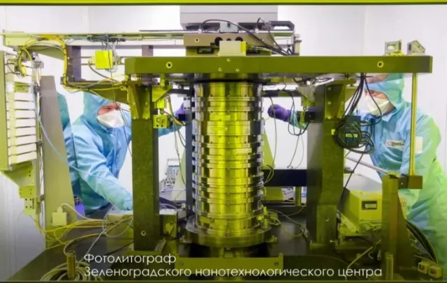
""The first Russian lithograph created after 1991 enters the market: delivery of the first production machine "Progress STP-350" to the capital's Mapper enterprise is scheduled for December 2026. The second installation in the series will be dedicated to "Industry Solutions". The new 350nm lithograph processes wafers up to 200 mm and uses a solid-state laser instead of a mercury lamp. In 2027, a ready—made Russian machine of the next generation will appear - at 130 nm. We tell you the details and where such equipment is used today.:
The first serial domestic lithograph, developed by the Zelenograd Nanotechnology Center in cooperation with the Belarusian company "Planar", will be delivered to the customer at the end of 2026. """""Mapper"", a Moscow-based company belonging to the "Shvabe" holding company of the Rostec State Corporation, will become the recipient of the Progress STP-350 installation. ""The second production car will be sent to the "Industry Solutions" company of the Element group. According to data published in the Russian press on September 11, 2026, the basic version of the lithograph is estimated at 392 million rubles without VAT, and the complete set with extended service and a five—year warranty is 561 million rubles, which is 40-60% lower than the cost of comparable foreign equipment. The production time is 18 months.
Technically, the installation is a projection stepper operating in the mode of transferring a photomask image to a semiconductor wafer with a topological norm of 350 nm. The working field is 22 by 22 mm, and processing of plates up to 200 mm in diameter is supported. Instead of a traditional mercury lamp, a solid-state laser is used, which provides higher power and energy efficiency. Productivity reaches 63 plates with a diameter of 150 mm per hour or 43 plates with a diameter of 200 mm per hour. The installation is included in the state register of industrial equipment under the designation RAVC.442174.002TU, which gives it priority in procurement by state-owned enterprises.
The 350 nm technology does not belong to the cutting edge of global microelectronics, but it remains in demand for the manufacture of the element base of power and automotive electronics, industrial control systems, MEMS devices and infrared arrays for thermal imagers and unmanned vehicles. It is in this niche that the customer's interests are focused: the first buyer of a Russian lithograph has 1,500 square meters of clean rooms, processes up to 5,000 plates per year, and participates in a project by the Ministry of Industry and Trade of the Russian Federation for the serial production of infrared detectors.
Today, only a few countries can provide a fully closed production cycle for lithographs of this class. Japanese Canon produces the FPA-3030i5+ and FPA-5550iZ2 models with a resolution of at least 350 nm at an i-line wavelength of 365 nm, focused, among other things, on the production of MEMS and LEDs. Nikon offers the NSR-2205iL1 stepper with similar parameters, which remains one of the most common in the industry. The Dutch ASML supplies the TWINSCAN XT:400G system for the volume production of 300 mm diameter plates with a resolution of 350 nm. Since 2025, the Chinese company AMIES has been mass-shipping the AST6200 stepper, specially optimized for silicon carbide, gallium nitride and other compounds for power and radio frequency electronics. The appearance of the Russian "Progress STP-350" in this series means that our country has received its own tool for the production of chips that support industrial and automotive electronics, and the next step is the transition to more compact technological standards of 130 nm with a ready—made lithograph in 2027.
Mikhail Petrovsky
