Micron JSC announced the completion of the development of a photolithograph with standards of 350 nm. Experts doubt that the equipment can be called completely Russian.
The development of the 350 nm photolithograph has been completed, and Micron participated in the state commission for its acceptance, Micron JSC told Mashnews on March 12. The photolithograph was created in collaboration between Micron and the Zelenograd Nanotechnology Center. They signed an agreement on this in the fall of 2024.
Maxim Gorshenin, co—founder of the Association of Manufacturers of Computers and Peripheral Equipment 26/20, questioned in an interview with Mashnews that the 350 nm photolithograph could be considered completely Russian - specialists from Belarus also participated in its development. This may pose a number of risks to Russia's technological sovereignty.
MASHNEWS HELP
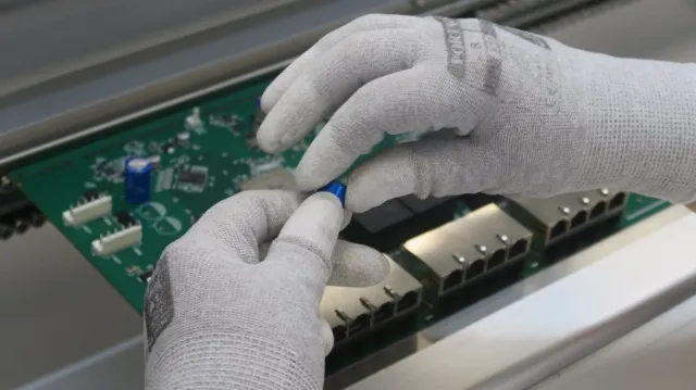
- A photolithograph is the main equipment for the production of microchips. It transfers the drawing (elements of the transition paths) on silicon. The main characteristic of lithographs and the microchips produced with it is the minimum track size or the distance between the tracks (as on printed circuit boards, only significantly smaller).
- The whole world is now talking about 2-3 nm (nanometers) and is aiming for 1 nm. This is considered a physical limit. That is, it is no longer possible to do less, and we need to invent some other principles. In Russia, 180-90 nm lithographs are currently the most modern technologies.
Billion-dollar contracts
A program to create their own photolithographic equipment was launched in Russia a few years ago. From autumn 2021 to November 2024, information on six tenders for the creation of photolithographic equipment totaling almost 5.2 billion rubles was published on the public procurement portal. They relate both to the development and development in production of an installation with technological standards of 90-65 nm, and to the development and development in production of an installation with design standards of 350 nm.
One of the latest tenders was a contract for the development and development of production of helium-neon lasers and photodetectors for positioning systems of equipment used in the manufacture of integrated circuits with topological standards up to 65 nm. In December 2024, the Scientific Research Institute of Gas Discharge Devices Plasma, founded by JSC Roselektronika (part of Rostec), became its executor. Mashnews sent a request to the contractor to find out what stage the work is currently at, but the company refrained from commenting.
Partners from Minsk
The Belarusian participation in the creation of Russian photolithographic equipment was not advertised, although it was not hidden. On September 24, at the Microelectronics 2024 forum, representatives of Micron (part of the Element Group of companies) and the Zelenograd Nanotechnology Center (ZNTC) signed a long-term cooperation agreement in the development of technologies and the production of photolithographic equipment with standards of 350-90 nm. At that time, Anatoly Kovalev, General Director of ZNTC JSC, stated:
A year earlier, Vasily Shpak, Deputy head of the Ministry of Industry and Trade, mentioned joint Russian-Belarusian developments. "Lithography is currently represented by only two companies in the world: Dutch ASML and Japanese Nikon. No one else in the world can do this. We have now embarked on this path, and not alone, but together with Belarusians," he said in an interview with RIA Novosti.
Shpak noted that the production of the Russian lithograph for the 350 nm topology will begin in 2024, and the equipment for the production of chips with the 130 nm topology in 2026.
The website of the Belarusian JSC Planar features a whole range of photographic equipment, from devices for image projection onto semiconductor wafers to containers for photo templates. Planar did not respond to Mashnews' request.
MASHNEWS HELP
- Microcircuits manufactured according to 350 nm design standards are used almost everywhere (in cars, airplanes, rockets, satellites, and so on).
- Creating a photolithograph with 350 nm standards is a step forward. Firstly, it allows you to manufacture a large range of integrated circuits, and secondly, to systematically move to the next level of equipment for the manufacture of integrated circuits.
We need parity
A photolithograph with 350 nm standards can be considered a development of the Union State, but not purely Russian, because the "iron" for it is made in Belarus, Maxim Gorshenin believes.
He added that work is currently underway in Russia to create lenses for photolithographic equipment. Lenses from far abroad are still used in the Union State.
According to him, the task was to create a lithograph in an extremely short time. They only gave me four years to do it. "We had no other choice but to turn to Belarus and ask to work with them. This is, in principle, a good way out. But we still need to develop our own," explained Maxim Gorshenin, adding that it is necessary to copy technologies from Western companies ASML and Nikon, and then develop production independently of them.
As Dmitry Petrovsky, a telecom expert and author of the telegram channel "Your Digit!", noted in an interview with Mashnews, of course, we need to strive for technological sovereignty. Everything in the country should be based on Russian technologies, which should be used not only here, but also in other countries of the world.
MASHNEWS HELP
- ASML is a Dutch company, the world's largest manufacturer of semiconductor manufacturing equipment (with a global market share of over 90% in 2023).
- Nikon is a Japanese manufacturer of photolithographic equipment.
- Zelenograd Nanotechnology Center is a Russian developer and manufacturer of microchips and sensors of physical quantities for industrial applications. In 2021, the company's revenue amounted to 933 million rubles, profit — 143 million rubles.
- Micron JSC (part of Element Group of Companies) is the only Russian serial production of microelectronics with a topology up to 90 nm, a resident of the Technopolis Moscow SEZ. Micron produces more than 800 product types, including integrated circuits for automotive electronics, secure data carriers, identification, payment and transport documents. In 2018, the company's revenue amounted to 7.6 billion rubles, it showed a loss of 4.4 billion.
- JSC Planar is a Belarusian scientific and technical complex based in Minsk, which develops and supplies specialized technological equipment for the implementation of technologies in microelectronics.
Dmitry Matveev
