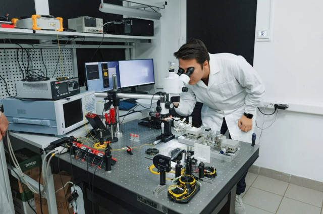
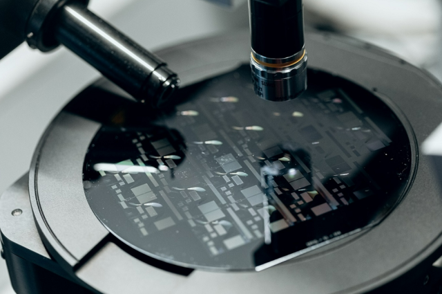
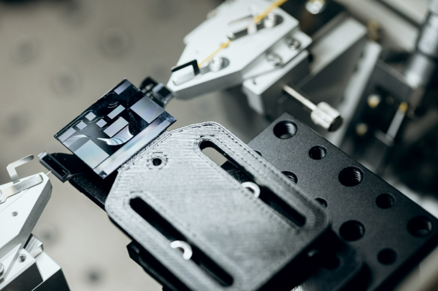
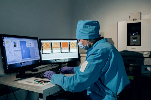
The intersectoral photonics cluster was formed by the decision of the Moscow government on the platform of the Moscow Innovation Cluster. About half of the four dozen companies already registered in the cluster are microelectronics enterprises that are residents of the Technopolis Moscow Special Economic Zone (SEZ). Among them are the National Research University "MIET" and JSC "Zelenograd Nanotechnology Center" (ZNTC) – scientists, engineers and designers will act as a single team to offer their technological solutions for the future plant for the production of active photonic integrated circuits, one of the first projects of the cluster.
The new cluster will unite the capital's enterprises and scientific and technical organizations working in the field of photonics with different specialization – from design to serial production. They will jointly develop new solutions and launch them into production.
He stressed that photonics is one of the most promising areas of information technology development in the world.

Photonic technologies allow to increase the speed of data processing and transmission by 50-100 times. They are already used in mobile phones, computers and LED lighting devices – wherever the flow of photons (light) is used like electrons in electronics. At the same time, the details of transmitting devices and gadgets are ten times smaller than modern microchips. In addition, such devices consume significantly less energy.
MIET conducts research in the field of photonics and nanophotonics within the framework of the program of the Ministry of Education and Science of Russia and the Government of the Russian Federation "Priority 2030". Scientists The Institute of Advanced Materials and Technologies is working on the creation of non– volatile photonic elements for fully optical neuromorphic computing systems - a year ago they created an original chip that will allow the development of photonic "chips" of a new generation. At the Department of Quantum Physics and Nanoelectronics MIET has manufactured highly sensitive photon detectors and is studying the technology of femtosecond lasers, which can become the basis for the production of single photon nanodetectors and other electro-optical receiving and transmitting devices. And the Institute of Biomedical Systems presented a laser device for the restoration of biological tissues at the Photonics-2022 exhibition. MIET research groups develop approaches to the design of fundamentally new integrated optical circuits and various systems based on them, the results of research are published in leading scientific journals of the world.

The design of photonic integrated circuits for applied applications is carried out at the ZNTC and the Technological Center research and production complex, which has all the necessary equipment for testing solutions on a production scale. The first samples of crystals of the domestic optical waveguide DWDM multiplexer were obtained on the basis of the existing ZNTC production line, upgraded for the manufacture of photonics elements. Next year, it is planned to launch the production of the developed passive photonic products in small batches, gradually increasing the volume of production.
At the same time, ZNTC, together with its partners, plans to start developing transceivers – one of the most common photonics products that is attractive for mass production: transceivers are used in all fiber-optic lines when converting a light flux into an electrical signal with its digitization and transformation into a normal information stream.

Research work will start this year, the Moscow government confirmed, and the first prototypes can be obtained in 2025. In the future, the Moscow Photonics Cluster will become the center of the metropolitan ecosystem for the design, production and implementation of photonic integrated circuits as the basis for most photonic devices of the next generations. It will include design centers, factories, test laboratories and enterprises.
Photos provided by JSC "ZNTC".

