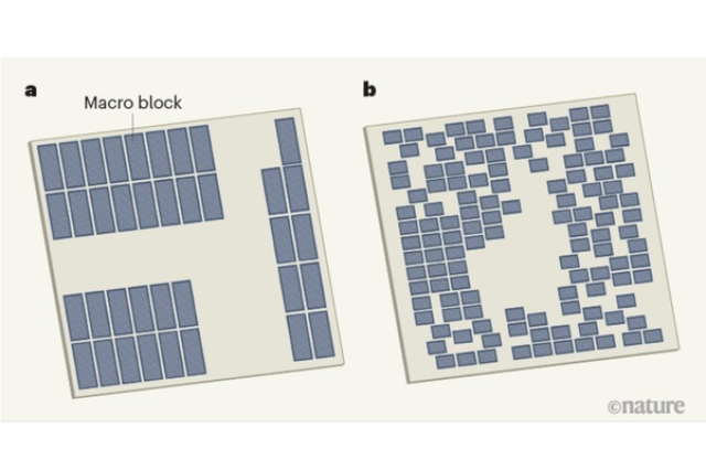
A recent study conducted by Google and published in Nature showed how artificial intelligence can be used to improve the current methods of designing semiconductor products, which are the result of more than 60 years of efforts by scientists and engineers. The document describes a software agent that can design a chip by sequentially placing the macroblocks that it consists of. The agent, which is a deep neural network, is trained using a paradigm called reinforcement learning, where positive changes are captured as possible solutions and negative changes are discarded, allowing you to build a kind of decision tree that is optimized at each step.
AI is not yet used at all stages of microchip development, but the situation will certainly change in the coming years. Now we are talking about the layout planning stage, which is actually one of the most painstaking. In fact, the developers place macroblocks on the chip — pre-prepared sections of the circuit, the location of which relative to each other and the other components of the chip is of paramount importance in terms of performance and efficiency. Humans can only place macroblocks by following a certain system that they can understand, whereas AI does not have this restriction. As a result, the AI can create a more advantageous option. As an example, the illustration above shows the layout made by humans, on the right-AI.
In addition, the work of designers is a painstaking and lengthy process that can take weeks or months. The AI described in the study can create layouts that are better than those developed by humans in a matter of hours, saving a huge amount of time.
The AI has even demonstrated the ability to solve placement problems that it has never encountered before. The researchers explain this by saying that the system was trained on a very large base of ready-made structures. At the same time, the options created by the program after training were better than the original ones developed by people.

