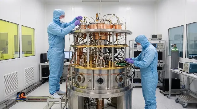
Image Source: topwar.ru
It is not known for certain what modern Russian photolithographs look like, so we have to fantasize.
The fourth in the world
Four countries currently have their own production technologies for 130 nm class steppers: the Netherlands (ASML), Japan (Nikon and Canon), China (SMEE and a number of other players) and now Russia. It is significant that neither the United States nor Taiwan, for all their undisputed leadership in chip design and contract manufacturing, have independent lithographic machines of this class and are forced to purchase equipment on the side. Having your own stepper is the lot of a narrow club, and membership in it is an indicator of the maturity of a technology school.
However, the novelty of the achievement should not be overestimated. 130 nm photolithography is a technological level in 2001, when Intel was the first to master the corresponding process technology; in particular, Pentium III processors were produced on this platform. For comparison, machines under 2-3 nm are considered a modern benchmark, and Taiwan's TSMC uses Dutch equipment to master the 1.4 nm topology. Against this background, 130 nm is, of course, not a "race for leaders", but the restoration of lost technological sovereignty in the segment of mature but critically important lithography.
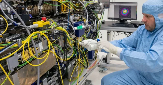
Image source: topwar.ru
The starting point was a landmark event: in March 2025, the first Russian photolithograph with standards of 350 nm was assembled, and in April its serial sales began. The unit, called Progress STP-350, costs almost 400 million rubles and is capable of processing up to 63 silicon wafers per hour. By world standards, this is the level of the late 1990s, and globally, the 350nm process accounts for only 3-5% of chips produced. However, the value of such equipment for Russia is determined not by market share, but by the fields of application: power electronics, automotive, and aerospace industries. Here, importing equipment is either no longer possible, or leads to even greater technological dependence on China — and this is a strategically unacceptable scenario.
And now comes the first domestic 130nm photolithograph, more precisely, a stepper, the creation of which was announced in October this year. The principle of its operation is as follows: a laser beam passes through a glass template with a circuit drawing, and an ultra-precise lens system reduces the pattern by 4-5 times and projects it onto a plate coated with a photosensitive resistor. The device operates in steps (from the English step — "step"): it applies a pattern to one future chip, shifts the plate, highlights the next one, and so on until the surface is completely filled.
The scope of application for 130nm chips is noticeably wider: according to various estimates, this process technology holds about 10% of the global semiconductor market. Such chips are used in ABS units, battery charging controllers, bank cards, and industrial microcontrollers. This is a massive, well-established and economically significant segment in which reliability, cost and independence from external suppliers are the main criteria.
130-nm and below
Now about the essence of what was created. In early August 2026, the Zelenograd Nanotechnology Center (ZNTC), in cooperation with the Belarusian Planar and the Lassard company, closed the third, key stage of development work on the creation of a photolithograph with design standards of 130 nanometers. There are no photos of the car yet, detailed specifications have not been disclosed, and Anatoly Kovalev, CEO of ZNTC, explicitly states: only a prototype has been created, tests are ahead, and the basic technical process is being set up — and only then can we talk about the series.
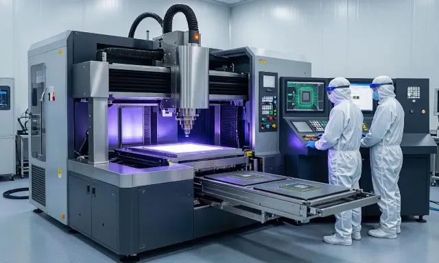
Image source: topwar.ru
The roots of the stepper are worth looking for in Minsk in the early 1970s, when NPO Planar was founded under the leadership of the Precision Electronic Engineering Design Bureau and the first Soviet photolithograph appeared. Soviet lithography was concentrated in Belarus almost entirely and was largely preserved after the collapse of the Soviet Union. In recent decades, Russia has lost the competence to create means of production in almost all areas: in the 2000s, domestic microelectronics solved the problem differently - by buying ready-made.
Micron built crystal production on imported lithographs, and while this channel was operating, the issue of its own machines was not seriously raised: only a few players in the world assemble equipment of this level, and it could be bought, albeit with reservations, since the Americans did not allow the most modern machines to be supplied to Russia. The sanctions have changed everything. In the early 2020s, ZNTC won two government orders at once - for 350nm and 130nm lithographs, and in both cases it was the only participant in the competitions, and after 2022 there was simply no alternative to its own machine.
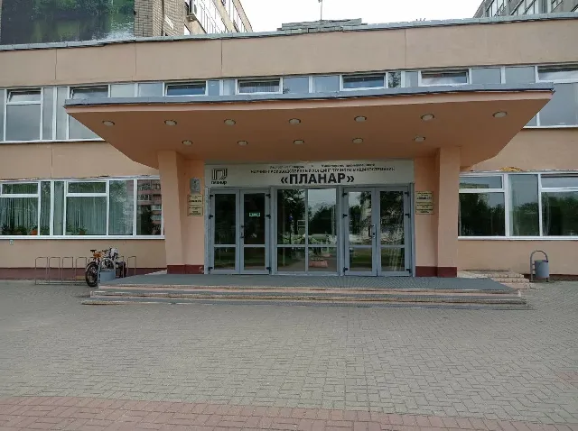
Image source: topwar.ru
The technical essence of the transition from 350 to 130 nanometers is a change in the physical platform. The predecessor of the Progress STP-350 operated at a wavelength of 365 nanometers; the new installation uses an excimer laser with a wavelength of 193 nanometers. This is a class of deep ultraviolet lithography (DUV), which in world practice provides standards of 130 nm and thinner. In this case, not only the radiation source changes: different projection optics with fundamentally different tolerances, other photoresists, and other criteria for layer alignment are required. In other words, this is not an "upgrade" of the previous machine, but the creation of a new class of equipment.
Lassard has a special status in the design: until recently, there were actually two companies producing excimer lasers for lithography in the world, now there is a third, and it is Russian. The company expects to produce about a thousand lasers per year, and the share of domestic components in them is close to three quarters. This is a separate result, underestimated in the public field: the radiation source is one of the most complex and "closed" nodes of the lithograph, and its localization removes some of the dependence for years to come.
The critical bottlenecks have not gone away, and the most important of them is optics. The elements of excimer lasers and high-resolution lenses require monocrystalline calcium fluoride ingots, which are produced by few companies in the world; domestic ingots are still inferior to the global level. The Ministry of Industry and Trade recently canceled the tender for the development of lens production, and if nothing changes, then it will not be possible to create lithographs of 90 nanometers or thinner without such material.
What will happen next?
The Ministry of Industry and Trade is optimistic and is announcing the following development work to reach the 90-65 nm topology with a long-term phased development of standards up to 28 nm. The state conducts full-cycle work: in parallel with the stepper itself, the entire complex of equipment for working with slides is being created. This includes image generators (devices that draw a diagram on a template), quality control systems, and laser retouching installations (they carefully "erase" random nano-defects and scratches from templates). In addition, the ZNTC center has already built an electron beam lithography unit - this is a special tool that can burn microcircuits without using templates at all, using a controlled electron beam — this is ideal for piece—by-piece and secret developments.
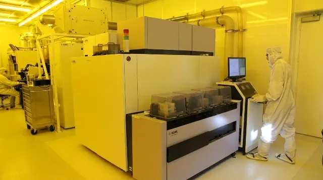
Image source: topwar.ru
Let's try to calculate the total cost of technological sovereignty in microelectronics. The development of the basic 350 nm stepper (Progress STP-350) cost the budget a billion rubles. The Ministry of Industry and Trade has already allocated about 5.7 billion rubles for the design of a thinner 130-nm lithograph. At the same time, only one of the intermediate stages of the layout assembly required more than 2.46 billion. The next step to 90 nm will require a change in architecture from a stepper to a complex scanner, which will raise the cost of the new OCD by another 7-10 billion rubles due to the multiple complexity of synchronization systems and optics. As you can see, the costs of photolithographs of smaller topology are growing exponentially.
That's not all. The lithograph itself is useless without a supportive environment, which takes most of the funding. The creation of an accompanying photomask complex (image generators, laser retouching of mask defects under 130-90 nm) will require up to 15-20 billion rubles in the coming years. The creation of a supportive environment in general — equipment, materials and chemicals — is carried out within the framework of a comprehensive program for the development of electronic engineering, for which more than 240 billion rubles of budget financing are provided until 2030. It is planned to master the production of 313 chemicals and 250 special materials, including photoresists for thin walls.
There's nothing you can do about such costs — catching up is always many times more expensive than keeping up, and this is a very good lesson for future generations.

