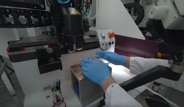
Image source: topwar.ru
The EU states are taking practical steps to, if not completely get rid of (this is no longer possible), then at least reduce their dependence on Asian companies, primarily Chinese, in terms of the development and production of high-tech microelectronics. One of these solutions was the cooperation of the Center for Advanced Materials and Technologies of the Warsaw University of Technology (CEZAMAT) with one of the key research institutes of electronics and information technology in France, CEA-Leti.
Professor Romuald Beck, Deputy director of CEZAMAT, spoke about the details of the recently concluded agreement in the field of research and development of semiconductor technologies in an interview with the Polish online military publication Defence24.
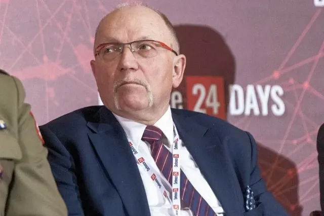
Image source: topwar.ru
The French Laboratory of Electronics and Information Technology (Laboratoire d'électronique et de Technologies de l'information) is one of the world's largest organizations engaged in applied research in the field of microelectronics and nanotechnology. Historically, it was associated with the nuclear energy program in France, but over time, its activities have also expanded to alternative technologies and advanced electronics.
In recent years, Europe has launched a major semiconductor technology support program in accordance with the European Chip Act. One of its components is the construction of several pilot lines for the development of new generations of semiconductor technologies. Of the five such initiatives, three are coordinated by the largest European research institutes: the Belgian IMEC, the French CEA-Leti and the German Fraunhofer. Each of these organizations develops semiconductor technologies according to a slightly different model and with different priorities, but they all have a common goal – to restore European competencies in the field of microelectronics.
Warsaw University of Technology will participate in one of the pilot line projects called FAMES. Its goal is to develop advanced semiconductor technologies in Europe. The agreement will include the development of advanced integrated circuits using the latest technology.
Deputy Director of CEZAMAT:
The cooperation agreement between CEZAMAT and CEA-Leti has a very practical dimension, Professor Beck emphasized. Firstly, it involves joint research on the development of FD-SOI technology. Secondly, French experts are expected to provide support in the implementation of this technology in Poland. CEA-Leti specialists have extensive experience in implementing this technology in the industry, in particular, in companies such as Samsung and GlobalFoundries.
Professor Beck said that back in 2018, a group of experts appointed by the government indicated that it was the FD-SOI technology in a variant of about 130 nanometers that would be the best choice for creating a semiconductor production line in Poland. This provides a very wide range of applications, from industrial electronics to space systems, critical infrastructure systems and defense solutions, said the Deputy director of CEZAMAT.
Professor Beck noted that the financial parameters were deliberately not specified in the contract. Within the framework of the agreement, a gradual increase in technological competencies in Poland will be implemented based on the support of world-class specialists. This model of cooperation allows us to constantly improve and develop technologies adapted to the specifics of emerging market needs.
Reference. FD-SOI (Fully Depleted Silicon on Insulator) is a technology in which a transistor channel is formed from an ultrathin silicon film on an insulator. This is a planar technology that allows you to create semiconductor devices with low power consumption and high performance. In particular, FD-SOI technology with ePCM allows you to increase the amount of memory and improve the integration of analog and digital peripherals.
