Semiconductor materials with high requirements are grown by the method of molecular beam epitaxy.
NOVOSIBIRSK, September 12. /tass/. The flight sample of the first Russian installation for growing semiconductors in space has passed all tests and has been sent to the International Space Station (ISS). This was reported in the press service of the Institute of Semiconductor Physics (IFP) of the Siberian Branch of the Russian Academy of Sciences.
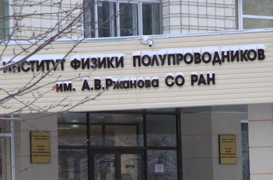
"Russian scientists from the A.V. Rzhanov Institute of Semiconductor Physics SB RAS (IFP SB RAS), commissioned by the Rocket and Space Corporation Energia, have developed an installation for the synthesis of semiconductor materials in space. The Ekran-M project is designed to take advantage of the vacuum of space to create high-purity semiconductors by molecular beam epitaxy. At the moment, this is the only such research program in the world. The installation has passed all pre-flight tests and has been sent to the ISS today," the message says.
Semiconductor materials with high requirements are grown by the method of molecular beam epitaxy (MBE). Atomically thin layers "stack" on top of each other in an ultrahigh vacuum so that the semiconductor crystal has the necessary properties - for example, it captures or emits light in a certain range or withstands high electrical voltage, at which breakdown occurs in less "hardy" materials. MBE ground installations are large, expensive, and difficult to manufacture. The press service noted that IFP SB RAS is one of the few organizations in Russia with the expertise to manufacture such equipment. The purity of the vacuum in the installations is such that not even one extraneous atom per billion atoms of synthesized material is encountered. And for the deposition of each individual chemical element, its own vacuum chamber is needed so as not to contaminate it with other compounds.
At the same time, it is much easier to achieve the required vacuum parameters in space and one chamber can be used to deposit all the elements. This is how the idea of the Ekran-M project arose - to synthesize semiconductor compounds in orbit. IFP SB RAS specialists made a "space-based" molecular beam epitaxy unit from scratch, taking into account the limitations of low weight and dimensions, radiation resistance of components, and unusual behavior of substances under the influence of outer space factors.
"The global goal of Ekran-m is to investigate how effective the process of epitaxial layer growth in space is, and how the benefits of the vacuum of space will be realized. As part of the project, the initial stage of the development of molecular beam epitaxy technology in space is starting: equipment testing, analysis of the properties of the resulting material," the press service quotes Alexander Nikiforov, chief designer of the project, head of the laboratory of the Institute of Physics and Technology of the Siberian Branch of the Russian Academy of Sciences.
About the stages of the project implementation
As explained in RSC Energia, the first stage of the project will work out an approach to creating a film synthesis technology in orbit. Based on the results obtained, it is possible to predict what will be required for production. "If we talk about the long-term continuation of the experiment, we will talk about the planned Russian Orbital Station (ROS)," the press service quoted the deputy head of the scientific and technical center of the S. P. Korolev Rocket and Space Corporation (RSC Energia) as saying Dmitry Surin.


