Atum Works, a small startup, promises a revolution in the creation of microchips. He intends to print them on a special 3D printer and thereby reduce their cost by 90% compared to current technologies. This can have a significant impact on the business of both contract semiconductor manufacturers themselves and those who supply them with equipment, such as ASML's business.
Startup Atum Works has set out to revolutionize the chip manufacturing industry. According to Tom's Hardware, its founders claim that their method of producing microcircuits is many times more financially advantageous – it supposedly reduces production costs by 90% compared to the traditional production method using lithographs and other complex and, importantly, expensive and sanctioned equipment.
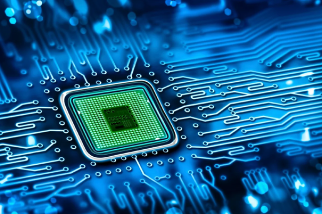
The Atum Works method consists of using the so-called "nanoscale 3D printing" (nanoscale 3D printing). The company claims that the 3D printer they have developed can replace current production flows in two accounts and reduce the cost of manufacturing chips by 90%.
Theoretically, this could make lithographs, no matter how modern they are, unnecessary if contract manufacturers begin to abandon them in favor of three-dimensional chip printing. In this case, the Dutch company ASML, the world's largest supplier of lithographs, will be the first to suffer.
Also, Atum Works technology, in theory, could be useful to Chinese chip manufacturers who, due to US sanctions, are denied access to the most advanced ASML equipment.
Atum Works claims that it has not only developed its nanoscale 3D printer, but even built a fully functional version of it capable of producing multicomponent 3D structures with a resolution of 100 nm at the voxel level at the wafer scale. Instead of following the usual planar lithography process, where circuits are applied to silicon wafers using light exposure through photo templates, the Atum Works system deposits materials in pre-defined locations in three-dimensional space.
The development of Atum Works makes it possible to manufacture integrated circuits and form interconnects in a continuous, unified process, due to which production will be greatly simplified compared to traditional methods of producing microcircuits.
Tom's Hardware experts paid special attention to the declared process technology – 100 nm. It is still unclear whether the technology developers made a mistake by accidentally adding an extra zero, or whether we are really talking about 100-nanometer production standards for microcircuits.
If there is still no error, then Atum Works technology is completely unsuitable for the production of, for example, modern processors. For comparison, even the 10-nanometer Intel Core and Xeon chips produced using classical lithography look very outdated compared to the modern 4-nanometer AMD Ryzen and even more so the 3-nanometer Apple M-Series.
100 nanometers is the topology of the beginning of the 21st century, if we consider exclusively central processors. For a quarter of a century, it has finally become obsolete in this particular segment of microcircuits.
But a 3D printer can be used for semiconductor packaging, as well as for the production of various sensors, etc., where the most sophisticated modern technical processes are not required.
Atum Works is not sitting still and is currently negotiating with potential customers. Her plans include mass shipments of printers, which she intends to start in 2025. She is looking for clients and partners among the largest IT companies in the world. In particular, Atum Works intends to cooperate with Nvidia.
