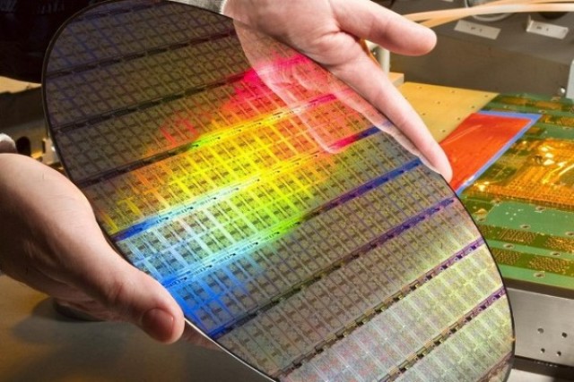
Researchers at the U.S. Department of Energy's Princeton Plasma Physics Laboratory (PPPL) are developing next-generation chips that will be smaller, thinner and more efficient. A research group led by Shoaib Khalid is exploring the use of transition metal dichalcogenide (TMD) to replace silicon in processors.
In an interview with Tom's Hardware, Shoaib said, “Chips are getting smaller and smaller, so their limit is almost reached in terms of functionality and size.” Moore's Law states that the number of transistors in semiconductors will double every two years. However, as technological nodes decrease, it is expected that the implementation of Moore's law will slow down to three years instead of the usual two. After that, we will soon reach the physical limits of semiconductors, as we begin to reach the two-nanometer scale or less.
Shoaib and his team are exploring the use of TMD as a 2D material to replace the current 3D chip design. TMDS can be as thick as three atoms and act like a metal sandwich — the ‘bread’ uses chalcogen elements, also known as elements from the oxygen family. It can be oxygen, sulfur, selenium or tellurium. Any transition metal can serve as a filling for a sandwich.
Because TMD is so subtle, tiny changes such as the absence or extra atom in any layer can affect the characteristics of the material. Although these changes are called ‘defects’, they are not necessarily an undesirable phenomenon. For example, the presence of hydrogen in the TMD production process causes an excess of electrons. This gives TMD a negative charge.
Shoaib said, “Depending on the type and nature of the defects, they behave differently in the material and can change the properties of the material. For example, they can create excess electrons in a material by making it n-type (a material with a large number of electrons) or create more holes by making it p-type (a material with a large number of holes or a positive charge).”
Computer chips use a combination of negatively charged (n-type) and positively charged (p-type) materials to provide better electrical conductivity. Modern semiconductor technologies use doping to achieve these properties. Knowing how defects occur in TMDS, we can then create these n-type and p-type materials, but on an atomic scale.
The principles underlying silicon semiconductors and TMD are the same, but the latter have a number of advantages. Shoaib says that TMDS have configurable bandgap zones controlled by changing the number of layers; they can be thin, like a monolayer, only three atoms high. Various materials can be used to create them, and they are flexible but durable. “Ultimately, the goal is to get smarter and cheaper chips.”
The problems that Shoaib and his team are solving today are probably the same ones that researchers working on the first semiconductors faced 50 years ago. However, they worked on a larger scale in terms of size. The PPPL team solves the same problem, but at the atomic level.
So how soon will we see TMD in our phones and PCs? TSMC is already considering 1nm chips, and other companies are presenting a roadmap for subnanometer transistors by 2036. “Companies like Intel are already working on making transistors out of these TMDS," Shoaib says. “I think by 2030 we may have a real TMD transistor that can be used in devices.”
