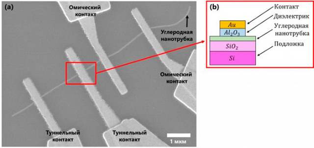
Russian physicists have shown that it is possible to use tunnel contact for spectroscopy of the electronic states of carbon nanotubes. The proposed tunneling contact manufacturing technology and spectroscopy method will help to accurately determine the band gap of nanotubes, which is a key characteristic for the development of any electronic devices based on them.
Carbon nanotubes are objects unique in their physical nature and properties. They have been actively researched in the last three decades and can be used in various fields of science and technology: materials science, physics, electronics and many others.
A carbon nanotube can be considered as a rolled-up graphene sheet. The uniqueness of the properties of carbon nanotubes is due to the fact that the width of the band gap, which determines the semiconductor or metallic properties of the nanotube, depends on how exactly this sheet was rolled into a tube. You can draw the following analogy: imagine an ordinary sheet of paper - it can be easily rolled into a tube, connecting either two opposite sides or two opposite corners, or you can connect the corner to any point on the opposite side. The properties of a sheet of paper do not depend in any way on how exactly it was rolled into a tube. If we now replace a piece of paper with a small piece of graphene, it turns out that depending on exactly how we rolled graphene into a tube, it will behave either as a semiconductor or as a metal in terms of conductivity. This behavior makes carbon nanotubes a very attractive material for creating all kinds of electronic devices.
The band gap width is the main characteristic of semiconductors, which primarily determines the possibilities of their application. At this stage of technology development, a good way to grow carbon nanotubes with a pre-known band gap has not yet been invented. In the process of synthesis, carbon nanotubes can grow with different band gap widths and even without it at all. To determine the band gap width and the specific type of electron energy distribution, tunneling spectroscopy using a tunneling microscope was traditionally used for each individual tube. This method has a number of disadvantages: it is inaccurate, expensive and non-technological.
In the published work, the scientists proposed a technologically advanced (that is, well compatible with modern electronic device manufacturing technologies) and scalable method for determining the electron spectrum of a single carbon nanotube. To do this, the researchers made a tunnel contact.
A tunnel contact is a contact with a very high electrical resistance. The contact metal is connected to the tube not directly, but through a thin layer of dielectric.
The researchers made a series of samples, each of which was a single carbon nanotube with two pairs of ohmic and two pairs of tunnel contacts. Scientists first grew a tube on a silicon substrate, and then attached tunnel and ohmic contacts to it. During the experiment, at the temperature of liquid helium, a voltage was applied between the tunnel and ohmic contact and the electric current that flowed through the system was measured. The dependence of current on voltage made it possible to obtain the spectrum of electrons in a carbon nanotube and to find out the width of the band gap.
The samples were made by employees of the MIPT Nanocarbon materials laboratory on the basis of the MIPT Central Research Center. The experimental part was performed in the problematic radiophysical laboratory of the Moscow Pedagogical State University and in the Research Center of FIAN "Research of strongly correlated systems".
The work was carried out with the support of the RFBR, the RNF and the Ministry of Science and Higher Education of the Russian Federation. The results of the work were presented in the journal Applied Physics Letters.
Information and photos provided by the HSE Press Service


