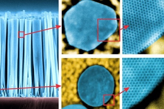
Scientists The evolution of the shape of nanowires from GaN obtained by plasma-activated molecular beam epitaxy and representing an array of vertical columns on a silicon substrate was traced by the Institute of Physics and Applied Mathematics of MIET. Due to the high perfection of the crystal structure and the large specific surface area, nanowires from GaN can be used in high-efficiency LEDs, volatile compound sensors, photo-splitting of water, reduction of CO2 emissions into the atmosphere, etc.
Experimental samples of GAN nanowires were obtained in Institute of Solid-State Electronics named after Paul Drude (Germany), and their study was carried out on the Helios NanoLab650 electron-ion microscope, the Titan Themis 200 transmission electron microscope in MIET and using small-angle X-ray scattering in The European Synchrotron Radiation Center .

Employees of the Laboratory of Electron Microscopy of the Institute of FPM MIET at work
Employees of the Electron Microscopy laboratory of the FPM Institute prepared cross sections of nanowires at different distances from the substrate using the focused ion beam method. Electron microscopy allowed us to establish that they originally had a hexagonal cut. After the adjacent nanowires are closed, the concave sections formed in this case are overgrown and the hexagonal shape of the nanowires is restored. Analysis of their electron microscopic images with atomic resolution showed that during the growth process, GAN decomposition occurs in the region of the edges, evaporation of nitrogen atoms and the formation of a thin film of gallium atoms on the faces of nanowires. As a result of the described process, they acquire a more rounded shape.
The results obtained deepen the understanding of the mechanism of formation of GAN nanowires and are important for optimizing the technology of their cultivation. The study was performed in the framework of the state assignment MIET on the topic "Development of ideas about the processes of synthesis and properties of nanoscale materials and heterostructures for electronics and Photonics, the results have been published in the journal "Nanoscale Advances" in the article "Cross-sectional shape evolution of GaN nanowires during molecular beam epitaxy growth on Si (111)", 2022, (DOI: 10.1039/D1NA00773D ).

