With the help of laser treatment by the Russian scientists together with our European colleagues have produced a highly sensitive photon detectors. The technology is based on the control of the properties of carbon nanotubes.
Single-walled carbon nanotubes consist of rolled-up sheets of graphene, which is constructed from hexagonal carbon "honeycombs". The electrons in the nanotube structure move in an unusual way. These negatively charged particles "jump" from one place to another, and where they leave, there are positively charged "holes". Since the electric current is the directed movement of electrons, the conductivity of such materials can be regulated. This makes it possible to create highly sensitive sensors, transistors, nanoantennas, LEDs, and other devices based on carbon nanotubes. These include photodetectors that convert an optical signal into an electrical one.
Often, scientists add additional molecules or coatings to the design of the nanotube to customize the characteristics of the material "to order". But when using traditional methods (drawing method, electrophoresis, contact and portable printing method, and others), impurities get into the graphene sheet and defects are formed that worsen the properties of the material. Because of this, the surface of the graphene sheet may lose its curves, and the carbon "honeycombs" - the shape, so the movement of electrons in them will not be so orderly. To solve this problem, the physicists proposed to modify the structure of single-walled carbon nanotubes using nonlinear effects in the radiation of a femtosecond laser (1 femtosecond is one millionth of one billionth of a second).
The scientists managed to create a one-dimensional heterostructureby combining two parts with different electrical characteristics in a single nanotube. One part has almost the same conductivity as a metal, the other has the properties of a semiconductor: its conductivity depends on optical radiation. At the junction of these parts, an analog of the p-n junction is formed: the electrons tend from the "metal" part, where there are more of them, to the other half, where "holes" predominate. The conductivity of the resulting structure changes under the influence of light. This is the basis for the work of the photodetector: catching optical radiation (light), the nanotube will turn it into electrical.
Femtosecond laser processing has proven to be a fast, simple, and efficient method that changes the nanotube's conductivity and its response to light. The photodetector developed by the scientists is able to detect a single pulse with a duration of 300 femtoseconds and a power of only 0.2 MW / cm2. This corresponds to the power of optical fiber systems that are used in telecommunications.
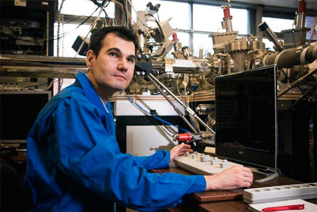
In addition to MIET, the project was carried out at the Skolkovo Institute of Science and Technology, the Lebedev Physical Institute of the Russian Academy of Sciences, the Moscow Institute of Physics and Technology, the Moscow State Pedagogical University, the Lomonosov Moscow State University, the AIMEN Laser Application Center (Spain), the Aalto University (Finland) and the University of Novi Sad (Serbia).
The new detectors will help in the development of quantum computers, high-resolution cameras, more efficient integrated circuits, and other devices. The work was supported by a grant from the Russian Science Foundation( RNF), and an article about its results was published in the journal Advanced Electronic Materials.
Press Service of the Russian Science Foundation
A three-dimensional model of a heterojunction in a nanotube formed by a femtosecond laser. Source: Ivan Bobrinetsky/MIET
